


ASML's Supply Chain, Bill of Materials, and the Devastating Effects of Potential Tariffs on US Fabs
A Forensic Analysis of the Lithography Monopolists Supply Chain and the Effect of Recent Tariff Policies

This article will deviate significantly from my other posts in that it will be much more technical in nature and the vast majority of it is AI-generated. I spent a good deal of time discussing the potential US tariff impacts on ASML with ChatGPT, and after crafting a comprehensive prompt, used the Deep Research feature to generate a detailed forensic analysis. This was initially intended solely for my own research and curiosity about the topic, but I found the report deeply insightful and wanted to share it with a wider audience.
Overall, the potential impact on tariffs is devastating and will involve significant trade-off decisions for US fabs. They will greatly increase the cost of lithography machines, which comprise the majority of fab spend, and will severely impact efforts to expand US capacity for chipmaking. Essentially, the tariffs will have the exact opposite of their intended effect of promoting domestic manufacturing capacity. Barring any specific exceptions for lithography machinery, these tariffs could effectively hamstring any potential for US competitiveness in chipmaking. The Trump administration is likely aware of this as industry giants like Intel and Micron will need to become deeply engaged in lobbying efforts to avoid this.
The entire analysis can be summed up with one sentence: ASML’s forensic supply chain mapping reveals a robust yet delicate web – one that global trade policies can perturb but likely not break.
With that, I hope you find this report as useful and insightful as I did. Since this is AI-generated, much of it comes from external sources, of which I’ve retained in-line citations. There are several other creators on Substack and other platforms that contribute deeply insightful analysis of their own.
ASML Supply Chain & Tariff Impact Analysis
Introduction
ASML Holding is the world’s leading supplier of photolithography systems, critical for manufacturing semiconductor chips (brief.bismarckanalysis.com). It is the sole provider of cutting-edge extreme ultraviolet (EUV) lithography machines and a dominant player in deep ultraviolet (DUV) lithography. In April 2025, the United States expanded tariffs affecting semiconductor equipment imports, introducing new complexities for ASML and its customers amid an evolving geopolitical landscape. This report presents a forensic analysis of ASML’s supply chain and a scenario-based assessment of how the April 2025 U.S. tariff expansion – alongside Chinese retaliatory moves and Dutch export controls – could impact ASML’s EUV (NXE series) and DUV (TWINSCAN/NXT series) business. We examine ASML’s multi-tier supplier network with country-of-origin mapping, the geographic distribution of its end markets (U.S., South Korea, Taiwan, China, Japan), and the potential effects on costs, demand, shipments, margins, and key customers. We also include historical context on ASML’s supply chain evolution, a technical deep dive into the Bill of Materials (BOM) of EUV and DUV tools, and scenario modeling projections of demand and risk by region.
ASML’s Global Supply Chain Breakdown
ASML operates a highly outsourced manufacturing model, relying on a vast network of specialized suppliers across multiple tiers. In fact, ASML outsources over 90% of its production to external suppliers (primarily in Europe) and serves as the master integrator of the final systems (wp.dig.watchwp.dig.watch). The company works with roughly 700 product-related suppliers, of which about 200 are considered critical single-source partners (ft.com) (semianalysis.com). Each EUV machine contains an astonishing hundreds of thousands of components (over 700,000 parts in the latest models), sourced from over 800 suppliers worldwide (quartr.comquartr.com). This distributed supply chain means that ASML directly employs only a fraction of the total workforce involved – less than half of the ~100,000 workers required to produce its machines are ASML employees, with the rest employed by its suppliers(economist.com). ASML’s role is to orchestrate and coordinate this network, acting as “the system architect” to integrate all the subsystems into one cohesive machine(wp.dig.watch). Below is a breakdown of key suppliers (Tier-1) and sub-suppliers (Tier-2/3) for major subsystems and materials in ASML’s EUV and DUV platforms, along with their country of origin:
Optics (Imaging & Illumination Systems): Carl Zeiss SMT of Germany is ASML’s long-standing strategic partner for optical components. Zeiss supplies the ultra-precise lens systems for DUV lithography and the multi-layer mirror systems for EUV (brief.bismarckanalysis.com). These optics require extreme precision; for EUV, Zeiss developed the “world’s most precise mirror” in collaboration with the Fraunhofer Institute in Germany (fraunhofer.defraunhofer.de). The optical materials come from specialized glass and crystal suppliers – e.g. Schott AG (Germany) provides purified optical glass and calcium fluoride crystals needed for DUV lenses. Each mirror or lens must be polished to atom-level smoothness and coated perfectly to reflect or transmit the desired light (fraunhofer.de). Zeiss’s optics have been core to ASML’s tools since the company’s founding, leading ASML to describe their relationship as “two companies, one business”(brief.bismarckanalysis.com). ASML even acquired a 25% stake in Zeiss’s SMT unit in 2016 to co-invest in next-generation optics R&D(brief.bismarckanalysis.com).
EUV Light Source (Laser-Produced Plasma): The EUV source is one of the most complex subsystems. Cymer (in San Diego, USA) – acquired by ASML in 2013 – designs the EUV source which fires 50,000 tiny tin droplets per second and blasts them with a high-powered CO₂ laser to generate 13.5 nm EUV light(zeiss.com) (wp.dig.watch). The high-power laser modules are supplied by TRUMPF (Germany). TRUMPF provides the “world’s strongest pulsed industrial laser,” a critical CO₂ laser amplifier with no economical alternative. Without TRUMPF’s lasers, the EUV source would not achieve the required output – as TRUMPF executives put it, “only TRUMPF can build the lasers needed for EUV lithography” (fraunhofer.de). This laser-driven plasma source also relies on high-purity tin (Sn) droplets (raw tin metal largely sourced from mining operations in countries like China, Indonesia, and Malaysia) and a hydrogen gas environment to mitigate debris. Key Tier-2 suppliers here include industrial gas firms (for hydrogen supply) and vacuum chamber specialists. The entire source module is largely assembled in the U.S. (Cymer’s facilities) and then integrated into the tool in Veldhoven.
DUV Light Source (Excimer Laser): For DUV (193 nm ArF excimer) scanners, the light source is also critical. Cymer (USA) is a leading supplier of excimer laser modules for ASML’s DUV tools, and Japanese firm Gigaphoton (Japan) serves as an alternative supplier for some customers (especially in Japan). These lasers consume specialized gas mixtures – notably Neon gas as a buffer medium. Neon (Ne) is a vital consumable for excimer lasers and has a concentrated supply chain: before 2022, about 45–54% of the world’s semiconductor-grade neon was purified by just two companies in Ukraine. The Russia-Ukraine conflict in 2022 halted roughly half the global neon output, highlighting a Tier-3 raw material vulnerability. ASML and its laser suppliers have since worked to diversify neon sourcing (e.g. from producers in the U.S. and China) (reuters.com). Other gases like fluorine are sourced from chemical suppliers in the U.S., Europe, or Japan. The excimer laser hardware itself uses optics (mirrors, electrodes) and electronics from various sub-suppliers in the U.S., Japan, and Europe.
Wafer Stage and Mechatronics: ASML’s scanners have sophisticated wafer handling and positioning systems. Dutch firm VDL ETG (Netherlands) is a key Tier-1 partner that co-develops many mechanical modules, including the wafer stage – a two-part stage that swaps wafers in and out and moves them beneath the lens at accelerations of up to 3⁰⁰g (three times the acceleration of a rocket launch) with nanometer precision. The wafer stage utilizes precision linear motors and air bearings. Magnetics and motion control suppliers (e.g. Philips Machinefabrieken or ASM Laser in Netherlands, Yaskawa or Mitsubishi Electric in Japan for servo controllers, etc.) contribute here. The linear motors use powerful neodymium-iron-boron magnets, which means rare-earth materials (mined largely in China) are embedded in the supply chain for the stages. For position measurement, laser interferometers and encoders from companies like Renishaw (UK) or Keysight (USA) are integrated to track stage position with sub-nanometer accuracy. VDL and ASML assemble these ultra-clean mechanics primarily in the Netherlands.
Electronics and Control Systems: Each lithography machine requires extensive electronics – from high-speed data processing units to precision analog controls for actuators. ASML works with numerous electronics suppliers: Prodrive Technologies (Netherlands) and Benchmark Electronics (US/NL) produce custom electronic modules; Intel FPGAs or Xilinx (US) chips might be used in control boards; high-performance computing units often use CPUs/GPUs from Intel, AMD or Nvidia. Ironically, the fabrication of these chips likely involved ASML’s own machines in customer fabs. Printed circuit boards and cabling may come from across the world (including some manufacturing in China or Southeast Asia for less critical boards). ASML has to ensure sensitive electronics meet strict cleanroom and reliability standards, often working closely with suppliers in developed countries.
Opto-Mechanical Modules: Some critical subassemblies, like the reticle (mask) handling system and the alignment/metrology modules, are built by ASML with help from specialty suppliers. Berliner Glas (Germany), which ASML acquired in 2020, supplies precision optical assemblies (it was a Tier-1 for things like wafer chucks and alignment optics). Jenoptik (Germany) provides optical components and modules for metrology. Hermes Microvision (HMI) (Taiwan), acquired by ASML in 2016, contributes e-beam inspection technology that complements lithography (though not a direct part of the scanner BOM, it’s part of ASML’s product portfolio for metrology).
Environmental Systems (Cooling & Vacuum): Lithography tools must maintain stable temperature, vibration isolation, and vacuum (for EUV). High-end vacuum pumps (e.g. from Pfeiffer Vacuum in Germany or Edwards in the UK) maintain the near-vacuum environment in the EUV beam path and source chamber. ASML’s “Hydrogen Catcher”: hydrogen gas is used in EUV sources to neutralize tin debris; gas handling systems are often custom-designed, with inputs from industrial gas suppliers (Air Liquide, Linde). Cooling systems circulate temperature-controlled water or refrigerants to dissipate the large heat loads (an EUV tool can consume 1MW+ of power including cooling). These cooling modules and heat exchangers are sourced from HVAC specialists in Europe. Vibration isolation platforms (to damp seismic or ambient vibrations) come from precision engineering firms like Newport or TMC (USA). All these environment-control subsystems ensure the machine operates within tight thermal and vibration budgets.
Raw Materials and Tier-3 Inputs: At the base of the chain are raw materials and chemicals: rare earth elements (e.g. neodymium for magnets, primarily mined in China), ultrapure silicon or quartz (for mirrors and windows, from suppliers in Germany, Japan, US), specialty coatings chemicals (for mirror multilayers – molybdenum and silicon thin films – often applied by Zeiss with tech developed alongside Fraunhofer (fraunhofer.de)). Tin metal for EUV (mined in Asia) and Neon gas (Ukraine/US/China) have been noted as critical materials. Additionally, the supply chain includes standard industrial materials (steel frames, aluminum modules, cabling, etc.) which might be sourced globally (Europe, Asia) but made to precise specs. The complex interplay is such that many parts cross borders multiple times during manufacturing – ASML’s CFO noted that components “get shipped back and forth several times between [Europe and the U.S.]” during production.
Overall, ASML’s supply chain spans three continents. Europe (especially the Netherlands, Germany, and to a lesser extent UK, France, etc.) provides the bulk of high-precision optics, lasers, and mechanical assemblies. The United States contributes key light source technology (Cymer), electronics, and software, and ASML employs about 20% of its workforce in the U.S. for engineering and manufacturing roles. Asia (Japan, Taiwan, South Korea, China) is mainly a market for ASML’s products, but also an indirect source of some components (e.g. Japanese suppliers for some materials and laser technology, and Chinese dominance in certain raw minerals). ASML’s business model is to coordinate this network such that all pieces arrive and are integrated into a finished lithography tool in Veldhoven (for EUV) or in its regional factories. This heavy reliance on specialized partners has been cultivated for decades – ASML calls it a “tradition of knowledge” cluster. The company maintains tight relationships, investing in or even acquiring suppliers outright when needed to secure technology (for example, ASML acquired Cymer to ensure EUV light source development, and warned other suppliers to cooperate or risk being bought out(brief.bismarckanalysis.com)). This strategy has yielded a resilient yet intricate supply chain that underpins ASML’s monopoly in EUV. However, it also exposes ASML to any trade disruptions affecting these supplier regions – a risk now under the spotlight with new tariffs and export controls.
Geographic Distribution of ASML’s End Markets
ASML’s customers are the world’s major semiconductor manufacturers, and its sales are geographically concentrated in a few key chipmaking hubs. Taiwan, South Korea, and China have been the top three countries for ASML’s sales in recent years, followed by the United States and then Japan. Each region’s demand profile reflects its semiconductor industry focus:
Taiwan: Home to TSMC (the world’s largest contract chipmaker) and other fabs, Taiwan has consistently been ASML’s #1 market. TSMC is ASML’s single largest customer – one of the “top two [that] account for ~60%” of ASML’s revenue(quartr.com). In 2023, Taiwan accounted for a substantial portion of ASML’s sales (roughly one-third or more). TSMC’s aggressive adoption of EUV lithography for 7nm, 5nm, and now 3nm nodes drove large orders of NXE series tools. For example, TSMC and two other firms even took a ~23% equity stake in ASML in 2012 to fund EUV R&D, underscoring the importance of ASML’s tech to Taiwan. Taiwan’s orders are primarily high-end: latest-generation EUV scanners and advanced DUV immersion tools for TSMC, plus some tools for other players like UMC or specialty fabs.
South Korea: South Korea is the second-largest market, thanks to Samsung Electronics and SK Hynix. Samsung (which makes both logic chips and memory) is a major EUV customer for its advanced DRAM and foundry logic lines, while SK Hynix (memory) uses primarily DUV immersion with plans for EUV in next-gen DRAM. South Korea generated about €6.4 billion of ASML’s revenue in one recent year. This was on par or slightly below Taiwan’s contribution. Samsung, along with TSMC, was an early investor in ASML’s EUV (part of that 2012 consortium). Thus, ASML ships multiple EUV scanners to Samsung’s fabs in Korea. Notably, Samsung and SK Hynix also have manufacturing in China (e.g. Samsung has NAND flash fabs in Xi’an, and SK Hynix has a DRAM fab in Wuxi). Those Chinese plants have continued to buy some equipment (mostly older-node tools) under special export license exceptions, which has indirectly made South Korean firms significant “China-based” customers as well. Overall, South Korea’s share of ASML sales has been typically in the 20–30% range, competing closely with China for the #2 spot in 2023.
China: In recent years, China’s share of ASML’s revenues surged dramatically, despite export controls. In 2023, Chinese customers accounted for 29% of ASML’s total sales – making China the third-largest market that year (and not far behind the top two). This spike was driven by Chinese chipmakers “flocking to buy older ASML equipment that does not face export restrictions” ahead of impending Dutch export license rules. Companies like SMIC, HuaHong, YMTC, and others bought as many DUV immersion and legacy tools as possible for mature 28nm+ processes. In Q1 2024, China’s buying spree peaked – a record 49% of ASML’s system sales that quarter (≈€2 billion) went to China as they raced to import tools before new rules took effect. However, going forward China’s share is expected to drop sharply due to export controls. ASML’s 2024 sales to China still ended up extremely high (an estimated 36% of sales in 2024 came from China (businessworld.in)), but with the new Dutch licensing in place (blocking shipment of ASML’s most advanced DUV tools to China from Jan 1, 2024), ASML projects China will fall to around 20% of sales in 2025. It’s important to note that ASML has never been allowed to sell EUV scanners to China – the US government has blocked export licenses since 2019. So China’s purchases are all DUV (KrF, ArF, and some older ArF immersion). This means China’s demand is mostly for 28nm and above processes, which are used in things like automotive chips, IoT, and older generation DRAM/NAND. With Chinese fabs expanding trailing-edge capacity as part of a self-sufficiency drive, China became a major consumer of ASML’s mid-tier tools until the recent restrictions. Despite geopolitical headwinds, ASML’s current CEO noted Chinese demand in early 2025 was “stronger than anticipated”, as Chinese companies continue to invest in mature nodes (which as of 2025 they can still mostly buy equipment for, except the very latest immersion tools). However, this demand is now tempered by uncertainty around how far restrictions will go.
United States: The U.S. traditionally has been a smaller share of ASML’s direct sales – roughly on the order of 10–15% of revenue in recent years (the U.S. was the fourth-largest region from 2020–2023, behind China). In 2022, for example, ASML had about 14% of sales in the U.S. Major U.S.-headquartered customers include Intel (logic), Micron (memory), and GlobalFoundries. Intel in particular is a key customer that is now ramping up EUV usage for its 7nm process (Intel 4) and beyond – Intel received its first EUV machine components for installation in Oregon in early 2024. As Intel and others invest in U.S. fabs (boosted by the CHIPS Act incentives), the U.S. demand for ASML tools is expected to grow in coming years. Additionally, TSMC and Samsung’s new fab projects in the U.S. (e.g. TSMC’s Arizona fab, Samsung’s Texas fab) will involve importing ASML lithography scanners. Thus, the U.S. market may climb in relative share. However, as we will discuss, the new U.S. tariff expansion in April 2025 puts additional cost pressure on these U.S. purchases. Notably, ASML also performs some manufacturing in the U.S. (in Wilton, CT and San Diego, CA), but those facilities largely produce modules rather than complete systems for sale. So the U.S. revenue figure mainly reflects machines shipped to U.S. fabs. From 2020–2023, the U.S. was behind China in ASML’s revenue ranking, underlining how much the center of chip manufacturing has shifted to Asia.
Japan: Japan represents a smaller portion of ASML’s sales (single-digit percent). Historically, Japanese chipmakers (like Toshiba/now Kioxia, Sony, Renesas, etc.) also bought lithography equipment, but Japan had domestic suppliers (Nikon and Canon) that dominated DUV lithography in earlier eras. In recent years, however, Nikon and Canon have fallen behind at the leading edge, and Japanese firms have started buying ASML’s latest tools for cutting-edge needs. For instance, Kioxia and Western Digital’s JV is adopting EUV for future 3D NAND flash production – ASML was slated to ship EUV tools for a Kioxia fab around 2024–2025. Also, a new Japanese consortium Rapidus (backed by the Japanese government to develop 2nm logic with IBM’s help) will rely entirely on ASML EUV scanners – Japan received its first EUV tool (an NXE:3800E) for Rapidus in early 2025 (rapidus.inc). These developments could increase ASML’s sales to Japan. In 2023, Japan was likely under ~5% of ASML revenue, but it is strategically important and closely allied with ASML’s home country regarding export policy. (Japan joined the Netherlands and US in aligning export curbs on advanced chip tools for China in 2023, given Nikon and Canon also produce some tools of concern.)
Other Regions: Europe itself has minimal leading-edge chip manufacturing, but ASML does have some European customers (like STMicroelectronics, Infineon, and Intel’s Ireland fab). These accounted for a few percent of sales (in 2022, Europe was ~1–2% of ASML sales (globalsmt.net)). Singapore (GlobalFoundries) and Israel (Intel’s fabs) also occasionally appear in sales by country breakdowns but are relatively small individually. The vast majority of ASML’s ~€21–28 billion annual net sales comes from the five regions above.
Summary: ASML’s revenue is heavily tied to Asia’s semiconductor hubs (around 80%+ of sales) with Taiwan, South Korea, and recently China being dominant. The U.S. and Japan are smaller but growing markets due to re-shoring efforts and new projects. This geographic mix means that trade policies in any of these regions can significantly affect ASML’s business. For example, China’s rush orders in 2023 (ahead of export controls) gave ASML a short-term boost, while the looming restrictions mean a potential drop in Chinese sales going forward. Similarly, U.S. tariffs could influence how ASML and its U.S. customers handle future equipment purchases. We next analyze the specific impacts of the April 2025 U.S. tariff expansion and related policy changes on ASML and its stakeholders.
Impact of April 2025 U.S. Tariff Expansion & Global Policy Responses
In April 2025, the United States implemented an expansion of tariffs that, for the first time, directly impacted semiconductor manufacturing equipment imports. Although the exact scope of the tariff expansion was broad-based, it included lithography machines and related components, effectively placing an import tax (reportedly on the order of 25%) on ASML tools shipped to U.S. customers. This move was part of a wider U.S. strategy to press China on trade and technology, but it had collateral effects on allied suppliers like ASML. ASML’s management acknowledged these tariffs as a new headwind: “recent tariff announcements have increased uncertainty in the macro environment” for 2025 and 2026. Here we assess the multifaceted impact:
U.S. Customer Costs and Purchasing Behavior
For U.S.-based chipmakers, the tariffs translate to a substantial cost increase on lithography equipment. An EUV scanner can cost in excess of $150 million each, and advanced DUV scanners tens of millions. A 25% import tariff would add tens of millions in tax per tool. ASML’s CFO Roger Dassen made it clear that ASML intends to pass most of these tariff costs onto the buyers rather than absorb them: “The burden of tariffs from our vantage point should be allocated in a fair way... those taking it in the United States should therefore take the lion’s share”. In other words, U.S. customers (like Intel, Micron, TSMC Arizona, Samsung Austin) will end up paying higher effective prices. This raises capital expenditure for U.S. fab projects, potentially altering purchasing decisions:
U.S. chipmakers might delay or reduce orders of new ASML tools due to higher costs. If a company had planned to buy, say, four EUV systems for a new line, the added tariff cost (potentially ~$30–40 million extra per EUV) could force them to re-evaluate the timing or quantity. However, since leading-edge lithography is usually not optional (to stay on technology roadmap), they may still purchase but look for other offsets.
Companies will likely lobby for relief or rebates. The CHIPS Act funding could be used to offset these tariffs indirectly (government incentives absorbing some cost). Industry groups have alerted that tariffs on semiconductor equipment could cost U.S. tool buyers over $1 billion per year in aggregate (in.tradingview.com). U.S. officials might consider exemptions or a refund mechanism for equipment destined for CHIPS-funded fabs, to ensure tariffs don’t undermine the very onshoring they are incentivizing. The ASML CFO suggested creating free trade zones or similar arrangements between the EU and U.S. to avoid double taxation on parts shuttling across borders. If enacted, such measures could alleviate some cost for U.S. buyers.
Procurement strategies may shift. U.S. customers might advance purchases before tariffs fully kick in (if there are grace periods on existing orders) or postpone hoping for a tariff rollback in future negotiations. They might also explore used equipment markets for certain older lithography tools (since tariffs on used vs. new might differ, or if they can buy from a third country). However, for state-of-the-art tools like EUV, the secondary market is essentially non-existent (no one sells their EUVs yet), so this is limited to older DUV.
Onshoring assembly: Another possible response is to ask ASML to perform final assembly in the U.S. (to classify the tool as U.S.-made). ASML already has significant U.S. operations and could, in theory, assemble some modules in a U.S. facility or a duty-free zone, delivering the tool within the U.S. without import (or with reduced duties on sub-components). This would be a complex logistical shift, but ASML mentioned free trade zones precisely because components cross the Atlantic multiple times. If ASML can designate a U.S. site for integration of certain systems, the tariff could possibly be sidestepped. However, this would take time to implement and might only make sense if tariffs look permanent.
In the short run, U.S. fabs simply face higher costs. This comes at a time when Intel, TSMC, Samsung are spending heavily on U.S. fab construction. A tariff effectively raises the cost of U.S. fabs relative to overseas fabs, potentially disincentivizing future expansion in the U.S. unless subsidies compensate. It’s a somewhat counter-intuitive outcome (trade policy colliding with industrial policy), and industry reactions have been negative. We might see U.S. customers push some tool deliveries into 2026 hoping the trade situation improves. Despite the friction, ASML noted that conversations with customers still support a growth outlook for 2025/2026 – the demand “remains very strong” due to AI and other drivers. This implies that leading chipmakers will likely stomach the cost (with help from government or pricing adjustments) to get the critical equipment they need.
Effects on ASML’s Shipments, Revenue, and Margins
From ASML’s perspective, the U.S. tariffs create uncertainty but may not drastically alter its top-line guidance, provided global demand stays strong. Key points include:
Near-term shipment volumes: ASML maintained its full-year 2025 revenue guidance (~€30–35 billion) despite the tariff news, suggesting they do not expect widespread order cancellations – rather a reallocation of cost. If a few U.S. orders are deferred, ASML might reshuffle production slots to other customers (for example, if Intel delays one EUV, TSMC or Samsung might be eager to get an extra one sooner). Global fab expansion plans (new fabs in Taiwan, Korea, Japan, etc.) can absorb some slack. In fact, ASML’s order backlog was around €38 billion in late 2023, so even if U.S. bookings slow, ASML has plenty of queued demand. However, ASML did see a drop in new bookings in early 2025 (net bookings €3.9B vs €5.4B expected) partly due to this uncertainty. Investors were concerned but relieved that 2025 guidance wasn’t cut. So shipments in 2025 may still grow, but the geographical mix could shift (fewer to U.S., more to Asia).
Revenue and Pricing: ASML plans to pass the tariffs to customers, effectively raising the selling price for U.S. deliveries. If that succeeds, ASML’s own revenue per tool (in euro terms) might even increase slightly (since the customer-paid price includes tariff). But practically, ASML will likely exclude the tax when reporting revenue and treat it as collected on behalf of government. The crucial point is ASML does not intend to grant discounts to offset tariffs – they “are ready to pass most of the tariff costs onto customers”. This stance protects ASML’s revenue and margins but at the risk of demand elasticity. U.S. customers have limited alternatives (ASML’s monopoly on EUV and dominance in advanced DUV means they can’t source equivalent tools elsewhere), so ASML has pricing power. This “hidden” pricing power was already noted by analysts – customers often pay large deposits and have few options. Thus, ASML’s revenue is more constrained by its production capacity and backlog than by pricing competition. We expect ASML’s gross margins to remain robust (~50%), as they will not voluntarily absorb tariff expenses. The CFO explicitly stated the tariffs should be “taken by those in the U.S.” rather than ASML. Unless political pressure forces ASML to share the burden, the company’s margin outlook stays intact.
Cost structure and operations: One area of impact is logistical complexity and potential extra costs for ASML’s own supply chain. Many of ASML’s suppliers are in Europe, but ASML does import some parts from the U.S. and possibly Asia that could be hit by tariffs either coming into Europe or going into the U.S. (depending on the exact tariff lists). If the U.S. tariffs apply to sub-components shuttled for repair or assembly, ASML might incur some taxes on parts moving between its U.S. and Dutch facilities. This could raise ASML’s manufacturing costs modestly. The suggestion of EU-U.S. free trade zones is aimed at mitigating precisely that: components that cross borders multiple times could otherwise be taxed repeatedly. ASML might adjust its supply chain routes or inventories to minimize dutiable transfers. In the long run, if tariffs persist, ASML could localize more production in each region to avoid tariffs – effectively a form of de facto supply chain decoupling. For example, certain subassembly manufacturing could be expanded in the U.S. for U.S.-bound tools. These moves would increase ASML’s operational costs (duplicate facilities, less efficiency), potentially squeezing margins a bit. However, such restructuring would be gradual. In 2025, the main direct effect is administrative: handling customs filings, paying tariffs then billing customers accordingly, and dealing with cashflow timing of those payments. ASML might also carry higher inventory if shipping through free trade zones.
In summary, ASML expects to weather the tariff impact with limited financial damage to itself (shifting costs to customers). The bigger risk is if tariffs undermine demand – but currently, chipmakers’ need for lithography seems inelastic for leading-edge nodes (AI chip demand, etc., is so high that fabs will proceed even at higher tool costs). ASML executives remain bullish that 2025 and 2026 will still be growth years despite the tariffs, as long as secular drivers (AI, 5G, automotive) fuel chip demand. They do caution that tariffs add uncertainty and could have indirect macro effects (if a trade war slows global GDP, that could dampen end-market chip demand). Another indirect effect: tariffs could spur more domestic competitors in the tool space if the U.S. government saw reliance on ASML as a strategic issue – but given ASML’s technological lead, this is a long shot. In fact, U.S. government seems satisfied using ASML as a “friendshoring” tool – leveraging the Dutch company to control China’s access to tech.
Chinese Retaliation and Policy Response
China’s possible responses to the U.S. tariffs and ongoing export controls can significantly affect ASML’s demand and supply chain. By April 2025, China was already limited in buying advanced tools, and the U.S. had further tightened export rules (notably NVIDIA’s $5.5 billion charge for restricted AI chip sales to China around that time). China has a few avenues to retaliate or adjust:
Accelerated Self-Reliance and Reduced Purchases: China may double down on domestic lithography R&D (through SMEE and other initiatives) and attempt to reduce reliance on ASML sooner. If Chinese authorities anticipate that even DUV tools will be choked off, they might scale back orders of any tools that are still allowed, instead channeling funds into indigenous equipment development – even if that means accepting lower yield or capability in the short term. A slowdown in Chinese orders would hit ASML’s shipment volumes. However, given China’s huge gap in lithography tech (SMEE’s most advanced scanner is only capable of ~90 nm to perhaps 28 nm in the future), completely cutting off ASML purchases would severely hamper China’s chip output. Thus, China is likely to keep buying any tools it legally can. Indeed, ASML noted Chinese demand for mature tools remained strong in early 2025. Retaliation in the form of an outright boycott of ASML is unlikely as it would hurt Chinese fabs more than ASML. Instead, expect China to prioritize orders for tools not yet banned (e.g. older immersion or KrF tools) until maybe they’re stockpiled.
Tariffs or Sanctions on U.S. Chip Equipment Firms: Since ASML is Dutch, direct tariffs on ASML from China wouldn’t apply (and China wants ASML tools). But China could retaliate against American equipment firms or chipmakers. For instance, China in 2023 had already banned certain products from U.S. memory maker Micron as a countermeasure. In 2025, China might impose heavy tariffs on equipment from U.S. vendors (Applied Materials, Lam Research, KLA) – however, those firms were already largely barred by U.S. export controls from selling advanced tools to China. So such tariffs would be mostly symbolic or affect only older equipment trade. If U.S. equipment companies earn less from China, they might focus more on other markets, indirectly helping ASML if overall chip capex is redistributed.
Retaliation via Material Supply Restrictions: A more direct lever China holds is its dominance in certain materials. China could restrict exports of critical materials used by the semiconductor industry – for example, rare earth elements needed for industrial lasers and precision motors (like neodymium magnets in ASML stages) or specialty metals (China has threatened export controls on gallium and germanium, used in chipmaking, and could extend to others). If China were to cut off or limit Neodymium magnet exports, ASML and its suppliers (which need these for motors) would face supply shortages or higher costs. There are alternative sources (e.g. Australia’s Lynas for rare earths), but ramping up non-Chinese supply takes time. Similarly, China could leverage its near-monopoly in some fluorinated chemicals or silicon wafers (China is a big producer of silicon wafer raw material). In July 2023, China already imposed export licensing on gallium and germanium – by 2025 it might extend to other inputs. If, say, high-purity quartz or certain lens polishing compounds from China became restricted, Zeiss’s production could be disrupted. Thus, Chinese retaliation might hit ASML’s supply chain indirectly by making certain inputs scarce. ASML would then have to find alternate suppliers (e.g. more Japanese or European sources for those minerals), potentially at higher cost. This increases supply chain risk and could inflate ASML’s production costs, impacting margins if not passed on.
Chinese Import Tariffs on Chips or Equipment: China could impose import tariffs on chips made with U.S. equipment or on equipment from specific countries. For example, they might threaten tariffs on chips produced by Samsung or TSMC in their China fabs using ASML tools, as a way to discourage compliance with U.S. controls. Such measures could reduce those companies’ incentive to continue production in China and thereby reduce ASML’s installed base service revenue in China. But these are speculative and would further isolate China’s tech industry, so they might be used only as a last resort if tensions escalate severely.
Compliance Challenges and Informal Pressure: Another response is that China could simply delay or deny certain service access to ASML. While ASML can’t ship new advanced machines to China, they still service existing ones. If relations worsen, China might make life difficult for ASML field engineers in China or impose bureaucratic hurdles, as a pressure tactic. This could hamper ASML’s Installed Base Management revenue (services/upgrades, which is ~25% of revenue(reuters.com)). However, ASML would still generally be allowed to support tools already delivered (the Dutch government was debating whether servicing falls under export controls). Any curtailment of service would in turn motivate Chinese customers to seek third-party maintenance or local solutions, which could reduce ASML’s future service income and insight into tool usage.
Overall, Chinese retaliation is likely to exacerbate the decline of ASML’s direct sales to China after the 2024 peak. ASML itself forecasted China’s sales portion dropping from 36% in 2024 to about 20% in 2025. In extreme scenarios of Chinese retaliation or further Dutch/U.S. curbs (e.g. if even mid-range DUV like 90 nm tools were banned), ASML could lose essentially all new system sales to China (which could have been 10–15% of business). However, ASML hopes other markets will compensate. Peter Wennink (ASML’s Former CEO) has often noted that if China can’t buy, the “demand doesn’t disappear – it just shifts”, as other global fabs will need to produce chips to fill the gap. For instance, if China can’t expand 28nm capacity, TSMC, GlobalFoundries or others may invest more in mature node capacity elsewhere, buying tools that ASML would have sold to China. Thus, the net effect on unit demand could be muted. The risk is if global trade tensions trigger a general economic downturn that lowers overall chip demand (hitting everyone’s capex, including TSMC, Samsung, etc.). ASML’s CFO warned that tariffs and export curbs have an indirect effect by potentially slowing global GDP and the “AI supply chain” growth. So, while Chinese policies might not directly crush ASML’s business (since others fill the void), they add systemic risk.
Dutch Export Licensing Constraints (and Allied Controls)
The Netherlands, under pressure from the U.S., implemented new export licensing rules as of September 1, 2023, which were fully enforced by 2024. These rules essentially ban ASML from exporting its most advanced DUV immersion scanners to China without a license. Since the Dutch government has signaled it will not grant such licenses for cutting-edge tools, ASML is effectively barred from selling any EUV (already banned) and now high-end ArF immersion tools to China. This policy directly caps ASML’s accessible market in China to older “mature” tools (like KrF lithography or older dry 193 nm systems). By April 2025, the Dutch and other allies were considering further tightening (e.g. Japan implemented similar measures for Nikon/Canon tools).
The impact of these licensing constraints on ASML includes:
Lost Sales and Backlog Adjustments: ASML had to remove or reallocate any orders from Chinese customers for advanced tools that can’t be delivered. The Reuters piece from March 2023 noted ASML had 14% of its sales in China in 2022. In 2023, Chinese firms front-loaded purchases of “mid-range” tools which were still allowed. From 2024 onward, ASML’s sales to China will be limited to older node equipment and service, significantly reducing potential growth. ASML stated it expects no material impact on its 2023/2024 financial outlook from these Dutch measures – implying it already filled the gap with other orders. But for the long term, missing out on what was nearly a third of the market (if unconstrained, China has enormous fab aspirations) is a strategic limitation for ASML.
Customer Mix Shift: ASML will rely even more on Taiwan, Korea, and the U.S./Japan for sales. If Chinese memory startups or foundries can’t buy immersion tools, competitors in Korea and the U.S. benefit (e.g. SK Hynix, Micron face less future Chinese competition in memory). But those competitors also then become more important customers for ASML. ASML’s customer concentration might increase (TSMC, Samsung, Intel taking an even larger share of orders). This concentration is already high – top 2 customers ~60% revenue – raising exposure if any of those big players fluctuate their investment.
Innovation and Services: ASML can still work with China on older tech, but China’s feedback loop on leading-edge requirements is cut off. Meanwhile, ASML’s R&D and supply chain adjustments might now deprioritize any China-specific features. Instead, ASML will coordinate closely with Dutch authorities to ensure compliance on service and spare parts. For example, questions like “Can ASML send replacement modules of an advanced immersion tool that was installed in China prior to 2024?” needed to be clarified. Likely they can, under service agreements, but the overhead of export control compliance has increased. ASML’s Installed Base revenue in China (currently significant because >100 DUV tools are installed there) could gradually erode if they cannot freely upgrade those tools. However, in 2025 ASML noted that many Chinese tools were still under service contracts contributing to about 25% of earnings from service worldwide.
Strategic Long-term Consideration: By excluding China from EUV and advanced DUV, Western governments are effectively forcing China to invest elsewhere or lag behind. If this strategy is successful, ASML doesn’t lose much because other countries build the capacity instead. But if it backfires (e.g. China manages to develop a domestic EUV alternative in, say, 10+ years due to necessity), ASML could eventually face a new competitor. As of mid-2020s, that threat is remote – ASML’s unique knowledge and its suppliers’ network took decades to build, and analysts deem it highly unlikely any competitor (Chinese or otherwise) can catch up without enormous investment and talent poaching (brief.bismarckanalysis.com). Still, ASML will carefully monitor any Chinese advances in 193 nm immersion tools, which could start eating into the low-end market if successful. In essence, export controls lock ASML out of a market, but also lock competitors (China) out of advanced tech, which maintains ASML’s near-monopoly globally (minus China).
In the broader context, allied export controls (U.S., Dutch, Japanese) serve to reinforce ASML’s strategic importance to allied nations’ chipmakers while denying that capability to China. The U.S. has explicitly used ASML as a linchpin in its tech containment strategy – “an effective means of restricting China’s access to cutting-edge chips, fulfilling a national security objective through ‘friendshoring’”(brief.bismarckanalysis.com). This geopolitical role means ASML must navigate between different government policies. The April 2025 U.S. tariffs, interestingly, put pressure on ASML’s allies (like Netherlands/EU) to possibly negotiate trade deals. If EU-U.S. trade tensions rise (the tariffs might be part of a dispute not directly related to chips), there’s a risk of misalignment: the Netherlands might question why it restricts sales to China at U.S. behest, only for the U.S. to then tax Dutch exports. So far, the Dutch remain aligned with the U.S. on security grounds, but trade frictions could strain that goodwill. If EU-U.S. relations soured, one could imagine the Netherlands being less stringent or slow-walking enforcement of export licenses as leverage. However, given the high stakes of semiconductor tech, such deviation is unlikely in the near term.
In summary, the April 2025 tariff expansion and ensuing policy moves create a complex picture: U.S. customers face higher costs but still need ASML tools; ASML itself aims to preserve margins by transferring costs and finds other buyers for any slack; Chinese demand, which temporarily buoyed ASML, will likely drop, but that capacity shifts to other regions; and ASML’s supply chain might need tweaks to mitigate tariff and retaliation impacts (like considering sourcing critical materials outside China and optimizing cross-border workflows). Next, we explore specific scenario analyses to quantify these effects and discuss how ASML and its customers might mitigate the associated risks.
Scenario Modeling and Risk Analysis
To evaluate the range of potential outcomes, we model several scenarios based on policy variables: U.S. import tariffs, Chinese retaliation severity, and export control stringency. We consider the impact on ASML’s unit demand (tool shipments), profit margins, and risk exposure by region and by customer. Each scenario also includes possible mitigation strategies (such as reshoring suppliers or dual sourcing) that ASML and stakeholders could employ. The scenarios are not mutually exclusive and could occur in combination:
Scenario 1: U.S. Import Tariffs on ASML Machines Persist
Assumptions: The U.S. maintains a ~25% tariff on lithography equipment imports through 2025 and 2026. No exemption is provided for semiconductor tools, meaning all ASML scanners shipped to U.S. fabs incur this tax. U.S. fab projects continue with CHIPS Act support, but equipment costs are higher. No additional escalation (tariff stays at 25%, and no counter-tariff by EU).
Impacts: U.S. customers will pay more per tool, potentially reducing the number of tools they can afford for a given capital budget. For instance, if Intel had planned $1 billion for lithography tools in 2025, a 25% across-the-board tariff effectively turns that into only $800 million of equipment buying power (unless supplemented). We might see U.S. orders defer ~20% of units relative to a no-tariff scenario. Concretely, if ASML would have shipped 50 tools to U.S. customers in 2025, perhaps only ~40 actually ship, with ~10 pushed to 2026 or canceled. This could shave a few percentage points off ASML’s global unit shipments (since U.S. was ~10% of sales, a 20% reduction there is ~2% global impact).
Financially, ASML’s gross margin might dip slightly if any tariff-related inefficiencies arise, but assuming ASML passes the cost, the gross margin could remain around 50%. Operating margin could face a bit more pressure if ASML invests in workarounds (like U.S. assembly sites) – perhaps a 1–2 percentage point hit due to duplication of effort or legal costs. Revenue for ASML might stay flat or even increase in euros because other regions take delivery of the tools not shipped to U.S. (backfilling from backlog). In fact, ASML stood by its growth forecast, indicating they can compensate for lower U.S. orders with others.
Customer behavior: Intel and Micron, heavily U.S.-based, become less cost-competitive per wafer vs. TSMC/Samsung (who build mostly in Asia without those tariffs). To mitigate this, the U.S. government might increase their subsidies to those companies. TSMC and Samsung might reconsider expansion scale in the U.S. – e.g. TSMC’s second phase in Arizona could be slowed, since importing many more EUV tools under tariff is expensive. Instead, they might concentrate new equipment in Taiwan/Korea unless political factors override economic ones. This scenario could ironically lead to fewer leading-edge tools in the U.S., keeping the bulk of advanced capacity overseas.
Mitigation: ASML would explore setting up a Free Trade Zone integration center in the U.S. If they can import subcomponents duty-free, assemble the tool in a FTZ or at customer site, and only assess duty on certain parts or not at all, that could greatly reduce the tariff cost. Another mitigation is negotiating a tariff exclusion – the semiconductor industry might successfully lobby the USTR for an exclusion on EUV and DUV tools (citing lack of U.S. alternatives, so tariff’s purpose to boost domestic industry doesn’t apply). If granted by late 2025, that would effectively remove the issue moving forward (this would shift us to a scenario of tariff removal). In the interim, cost-sharing arrangements between ASML and customers might occur – e.g. ASML could give slightly better payment terms or training credits to soften the blow (without formally reducing price, to avoid setting precedent).
Risk exposure: U.S. market risk is moderate – the main risk is project delays. If, say, Intel delays its EUV purchases by one year, ASML might have a gap, but TSMC or Samsung could fill it. The strategic risk is low because U.S. will eventually need those tools to meet its capacity goals. So this scenario is a manageable short-term dip for ASML, largely mitigated by global demand. The bigger risk is political: if tariffs cause enough pain to U.S. companies, it might strain U.S.-EU relations or cause U.S. policymakers to intervene in how ASML operates domestically (though that’s unlikely).
Scenario 2: Escalating Chinese Retaliation
Assumptions: Frustrated by U.S. tariffs and tech blockade, China undertakes strong retaliatory measures. It imposes export restrictions on critical materials (e.g. a 2025 ban on exports of rare earth magnets and certain specialty materials used in lithography equipment). It also perhaps ends all Chinese state-owned fab purchases from ASML as a form of protest (even of allowed tools), accelerating investment in domestic tool makers. Meanwhile, China levies tariffs of its own (say 25%) on any foreign-made semiconductor equipment, making ASML’s remaining legal sales in China more expensive.
Impacts: This scenario is more severe for ASML’s supply chain. A Chinese ban on rare earth magnets would disrupt the supply of key components like stage motors and laser amplifiers. ASML and suppliers would scramble to qualify alternate sources (e.g. higher-cost non-Chinese magnets from Japan or U.S.). During the transition, component lead times could increase, potentially limiting ASML’s production throughput. In a worst case, if certain high-performance magnet grades or optical coatings (China refines some optical coating materials) become unavailable, ASML might have to redesign some subsystems to use substitute materials. That could slow deliveries or reduce tool performance temporarily. ASML would likely stockpile critical materials pre-ban (once such retaliation is anticipated), mitigating short-term effects. Over 6–12 months, alternative supply chains (Australian rare earths processed in EU/US, etc.) could come online, but possibly at higher cost. ASML’s cost of goods sold would rise – e.g., magnet costs could double if not sourced from China. This could shave a few points off gross margin if ASML can’t immediately pass those increases on. However, given strong demand, ASML might raise tool prices marginally to offset new costs (chipmakers might accept that given the circumstances).
If China also pulls back on purchases of even mature tools, ASML’s system sales to China could drop to near-zero. For example, instead of contributing ~20% of 2025 revenue, China might fall to <5%. That’s a loss of perhaps €5–6 billion in annual sales relative to 2024. In the near term, ASML could partially fill that gap: TSMC, Samsung, Intel might gladly buy some of the tools that would have gone to SMIC or HuaHong (for mature nodes, global demand for chips like auto MCUs and power chips is strong, so capacity will be added somewhere). But not all tools are fungible – Chinese orders were often for older models; TSMC and others mostly want latest models. ASML might end up producing fewer total units in 2025/26 if Chinese orders vanish and not all are replaced one-for-one. We could see, say, a 10% drop in total unit shipments compared to projections, until other markets absorb the slack. Over a couple of years, other countries (including potentially India or Southeast Asia if they build mature fabs) could take up most of that volume.
ASML’s service business in China would also suffer in this scenario. If Chinese fabs can’t rely on getting new ASML tools or support, they may resort to cannibalizing parts and using local third parties. Over time, ASML might have to withdraw some service personnel if hostilities increase (political or legal barriers). The installed base could degrade, and ASML might write off some service revenue expectations. But service to China was perhaps ~10% of ASML revenue; losing half of that would be a 5% hit, not catastrophic for the company overall.
Mitigation: ASML would fast-track its supplier diversification programs. They have already been working with suppliers to reduce geographic concentration risk. In response to Chinese material restrictions, ASML could help fund new facilities – for example, fund a rare earth magnet production in Europe or partner with U.S./Japanese firms like Hitachi Metals or Vacuumschmelze to boost non-Chinese output. They might build larger safety stockpiles of critical consumables (gases, minerals) in safe locations. ASML could also redesign some components to use less scarce materials – e.g., use electromagnetic actuators that use electromagnets (copper-based) instead of permanent magnets in a pinch, albeit with performance trade-offs. For lost Chinese sales, ASML’s mitigation is to market aggressively to other emerging players – for instance, if China is off-limits, focus on new government-backed fabs in India (which has plans for foundries), Vietnam, or the Middle East where demand for mature-node tools might pick up with government support. Essentially, ASML would pivot to any region not restricted.
Risk exposure: This scenario heightens supply chain risk for ASML – the company would be more directly exposed to bottlenecks for certain materials. It tests ASML’s resilience. The financial risk is moderate: losing the China market beyond what’s already expected could reduce ASML’s growth trajectory. Instead of, say, 15% CAGR through 2025, ASML might see flat or low growth in that period if replacements don’t emerge. But ASML has such a technological moat that once global demand rebounds, it can recover. The strategic risk is that China, by cutting itself off, might more rapidly develop its own lithography ecosystem which in a decade could compete. However, in the short term, China would face immense pain – effectively halting progress at 28 nm. That likely ensures that at least some level of engagement with ASML remains in China’s interest (for mature tools).
Technical Deep Dive: EUV vs DUV System Architecture
Understanding the technical architecture of ASML’s lithography systems illuminates why its supply chain is so specialized and why these machines are so sensitive to supply chain and policy disruptions. We will dive into the BOM (bill of materials) and design of ASML’s EUV (Extreme Ultraviolet) scanners versus its DUV (Deep Ultraviolet) scanners, highlighting critical subsystems like the laser-produced plasma source, optics, wafer stage, metrology, and cooling modules. Each of these parts must perform near the limits of physics, and their origin often traces to a single expert supplier (as described in the supply chain section).
EUV Lithography System (NXE Series) Architecture
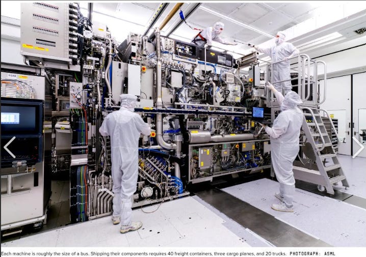
An ASML EUV scanner (such as the NXE:3400C, used for 7nm/5nm production) is often dubbed “the most complex machine humans have built” – weighing ~180 tons, costing over $150 million, and requiring a decade of R&D collaboration to realize. Its key subsystems include:
Light Source (EUV Excimer Laser Plasma): The EUV light source is a marvel on its own. It begins with a CO₂ laser (from TRUMPF) generating a high-energy beam (upto 30 kW of infrared power). This beam is focused into a vacuum chamber where tiny droplets of tin (Sn) (around 30 microns diameter) are being sprayed at ~50 kHz frequency. Each droplet is hit by a pre-pulse laser to flatten it and then by a main pulse laser, converting it into an extremely hot plasma that emits EUV radiation at 13.5 nm wavelength. The conversion efficiency is low – most energy goes to heat. The EUV photons radiate in all directions; a collector mirror (a large multilayer concave mirror from Zeiss) nearby gathers as much EUV as possible and directs it into the scanner optics. Generating EUV this way was so challenging that for years many doubted it was practical. It requires precise synchronization of droplet and laser (to within nanoseconds). The TRUMPF laser is the only one of its kind, delivering pulses on the order of 20 mJ at 50 kHz, making it the most powerful pulsed industrial laser globally. The tin supply and debris handling is also complex: a tin recirculation system collects unused droplets and debris using a combination of gravitational traps and a flowing curtain of hydrogen gas that helps clear sputtered tin. The hydrogen gas binds with tin vapor to form SnH₄, which deposits on a cold trap, preventing tin from coating the mirrors. Without this, the collector would be contaminated quickly. The entire source module is under vacuum and contains plasma-facing electrodes, spectroscopy sensors (to monitor EUV output), and mechanisms to adjust droplet trajectory. In summary, the EUV source is a self-contained subsystem roughly the size of a small car, bolted onto the main scanner. It’s supplied largely by ASML’s Cymer unit with parts from Trumpf and Zeiss.
Illumination Optics: Once the raw EUV light is collected, it enters the illumination optics module. Unlike DUV, which can use refractive lenses, EUV at 13.5 nm is absorbed by all materials, so it can only be manipulated by mirrors in a vacuum. The illumination optics (designed by Zeiss) consist of several multi-layer mirrors that shape and direct the beam to uniformly illuminate the photomask (reticle). These mirrors have to be precise in figure (shape accuracy on the order of picometers) and coating. They are coated with dozens of alternating layers of molybdenum and silicon (each about 7 nm thick) which create a Bragg reflector tuned to 13.5 nm. Each mirror reflects ~70% of incident EUV; with a cascade of 6-8 mirrors in the optical path, the transmission is only a few percent from source to wafer. Thus, the source must be extremely powerful to overcome losses. The illumination system includes a field facet mirror (to homogenize light) and an aperture to define numerical aperture and field size. There are also dynamic optical elements to adjust for dose and uniformity. Even the slightest contamination on these mirrors (like a particle or tin deposition) can ruin the optics, hence the importance of the vacuum environment and the hydrogen flush. The mask (reticle) itself is a special mirror: a quartz substrate with an EUV-reflective coating patterned with the chip design. It reflects the EUV (whereas in DUV the mask transmits light). The mask is held in a mask stage that can adjust its position and also has a protective pellicle – a thin, transparent (to EUV) membrane that shields it from particles. Developing an EUV pellicle was a huge challenge; current pellicles use ultrathin carbon-based films and absorb ~10-20% of EUV, further reducing efficiency.
Projection Optics (Imaging System): After reflecting off the mask, the EUV light carries the circuit pattern and goes through the projection optics – a series of high-precision mirrors that demagnify (4× reduction) and focus the image onto the wafer. The NXE:3400 series uses a 0.33 numerical aperture (NA) optics system with 6 mirrors (called the Schwarzschild optics design). These mirrors, also from Zeiss, are the most precise ever made. Any “irregularities [even] the size of an atom” on these mirrors would degrade imaging, so Zeiss and Fraunhofer spent years perfecting ion-beam polishing and coating to achieve picometer-level smoothness. The last mirror in the system is the objective that focuses the reduced image onto the wafer plane. Because of reflective optics, the system has to correct for distortion and aberrations by slight adjustments and mirror shaping. The entire optics module is mounted in a metrology frame isolated from vibrations. It also includes various sensors (alignment scope, phase gratings, etc.) to ensure the mask and wafer are aligned to an accuracy of a few nanometers.
Wafer Stage and Chuck: The wafer (typically 300 mm silicon) sits on a electrostatic chuck on the wafer stage. The chuck clamps the wafer via electrostatic force and also manages wafer temperature (via helium cooling under the wafer) because any thermal expansion can cause pattern distortions. The wafer stage is a dual-stage design in ASML’s “TWINSCAN” architecture: while one wafer is being exposed in the exposure position, another wafer on a second stage is at the metrology position (being measured and aligned). The two stages swap roles to maximize throughput (this dual-stage concept was a key innovation that gave ASML a lead in the early 2000s). The stage must move the wafer underneath the projection optics following a scan motion that is synchronized with the mask movement (the mask stage moves a smaller distance but 4× faster, due to the demagnification ratio). The speeds and accelerations are extreme: wafer stages reach acceleration ~30 m/s² (3 g) and velocities of 1–2 m/s over short distances, then decelerate precisely. This is needed to scan a ~25 mm × 33 mm exposure field in a fraction of a second. The positioning accuracy is better than 2 nm, maintained by a laser interferometry system that tracks the stage positions in real time. To achieve frictionless motion, the stages float on a magnetic levitation or air bearing system. They are driven by linear motors (Magnet arrays and coil assemblies) that allow swift, precise movement. The stage motion is so fast that if not properly controlled it could cause vibrations; ASML engineered counter-mass systems that move in opposite directions to cancel out forces. The entire stage apparatus is in vacuum (for EUV) and requires extremely flat stability. Components like the granitic base and vibration dampers in the frame come from specialized mechanical suppliers (which must ensure no deformation at the nanometer level during moves). Overall, the wafer stage is one of the most expensive mechanical parts of the tool, showcasing precision mechanics and controls.
Metrology and Control Systems: An EUV scanner incorporates a suite of metrology systems to measure and correct errors. Alignment sensors (using microscopes and lasers) measure the wafer’s alignment marks and the mask’s alignment to ensure correct overlay of patterns layer to layer. ASML uses its ATHENA alignment system (for EUV, a multi-wavelength approach because EUV itself is hard to use for alignment due to lack of pellicle transparency). The system builds an accurate model of wafer distortion and fine-tunes stage positioning accordingly. Additionally, focus sensors measure the wafer surface topography (heights) to adjust focus in real time (the wafer stage has a Z-actuator and tilt to maintain the wafer at the best focus plane despite any surface height variation). There are also dose monitoring sensors to track the EUV intensity and adjust for any fluctuations shot-to-shot. All these metrology feedback loops feed into ASML’s real-time control computers, which make tiny adjustments on the fly – e.g., tweaking mirror positions, laser pulse energy, or stage trajectory – to correct any deviations. An EUV scanner thus is not a static machine but an active mechatronic system with nanosecond and nanometer-level feedback control. The software that ties this together (ASML’s control software and computational lithography optimizations) is a crucial part of the system’s performance. ASML also offers computational lithography support (like scanner tuning and OPC – optical proximity correction – integration) to maximize the effective resolution and pattern fidelity.
Cooling and Environmental Control: The heat loads in an EUV machine are immense. The CO₂ laser dumps heat; the plasma radiates not just EUV but also significant thermal energy and debris. The mirrors absorb some EUV and IR energy. To manage this, the machine has multiple cooling circuits: water-cooled plates around the source, active cooling in mirror mounts, and the wafer chuck temperature control. The climate control inside the tool is also vital – any air (for DUV sections) must be ultra-filtered; in EUV vacuum sections, outgassing from materials must be minimized (all components are baked to remove volatiles that could otherwise deposit on mirrors under EUV radiation). The machine’s internal atmosphere is either high vacuum (EUV path) or purged with ultra-clean dry air or nitrogen (around stages, etc.). Temperature stability is critical: the entire body of the tool is maintained to within a fraction of a degree to avoid thermal expansions. The enormous power draw (some EUV tools can require >1MW including cooling infrastructure) means ASML often supplies a dedicated cooling rack and power conditioning unit with the tool. The facility interfaces (like vibration isolators that connect the tool to the fab floor) are also part of the system – isolating seismic or building vibrations using dampers and active feedback (some use interferometers to measure floor vibration and cancel it).
To summarize an EUV scanner’s operation: tin droplets + CO₂ laser produce EUV light, which is bounced through 11 or more precision mirrors in vacuum (collector + illuminator + mask + projection optics) to print tiny patterns on a wafer moving at breakneck speed, all the while correcting for errors in real time. The challenges overcome include plasma physics, optical coating science, ultra-precision mechanics, and control software – a confluence that only ASML and its partners (Zeiss, Cymer, Trumpf, etc.) have mastered. This complexity also means EUV tools are fragile in the face of supply chain issues: each of those specialized components (e.g., the Zeiss mirror or the Trumpf laser module) is largely single-sourced. That’s why export controls on EUV were so effective – no alternative source exists for China or anyone else; ASML’s EUV system is unique.
DUV Lithography System (TWINSCAN NXT Series) Architecture
ASML’s DUV scanners (such as the TWINSCAN NXT:2000i or NXT:2050i, used for 28nm, 14nm, and with multi-patterning even 7nm) share some architectural principles with EUV tools but also have distinct differences. DUV tools use 193 nm deep ultraviolet light generated by excimer lasers, and they use refractive lenses rather than mirrors. They operate in a mix of air and liquid immersion environments rather than full vacuum. Let’s outline a DUV immersion scanner:
Light Source (193 nm Excimer Laser): A DUV scanner typically uses an ArF (argon fluoride) excimer laser emitting at 193 nm. Cymer (ASML) and Gigaphoton make these lasers. The laser fires in pulses (e.g., 4–6 kHz pulse rate). Each pulse has high energy (mJ range) and is shaped to a short duration (~20 ns). The output is a deep UV beam delivered via a beam delivery unit (full of mirrors and noble gas purging) to the scanner. These lasers require a gas mixture of argon, fluorine, neon, etc. Neon, as mentioned, is a critical buffer gas that comprises most of the gas volume and must be ultra-high purity. Each pulse of the excimer laser discharges through the gas, producing intense UV light by exciting ArF molecules. The laser chamber consumables (gas, electrodes) need regular maintenance – part of ASML’s service business. The 193 nm light then often goes through a beam expander and homogenizer to create a uniform illumination field.
Illumination and Reticle Stage: The 193 nm beam enters the illumination optics module, which consists of lenses (often fused silica or calcium fluoride elements from Zeiss) and diaphragms to shape the beam’s angular distribution (offering different illumination modes like annular, dipole, etc., which enhance imaging of different pattern types). Because air absorbs 193 nm somewhat and can cause wavelength fluctuation due to humidity, the illumination optics is typically in a purged atmosphere (nitrogen purging) or a sealed environment. The light then hits the photomask (reticle), which in DUV is a quartz plate patterned with chrome (or phase-shift patterns) – essentially a stencil that either blocks or phase-shifts the 193 nm light in regions to create the pattern’s image via diffraction. The reticle is held in a reticle stage that moves slightly to synchronize the scanning (similar to EUV, the reticle moves as the wafer stage moves, since these are scanning projection systems, not full-field). The reticle stage is also precisely controlled but since it’s lighter (a thin plate), it’s easier to move quickly. Typically, it’s moved by a short-stroke stage and a long-stroke stage combination, analogous to wafer stage.
Projection Optics (Reduction Lens): After the mask, the image is projected onto the wafer by a projection lens system. This is one of the most critical parts of a DUV scanner. Built by Zeiss, it consists of a column of large lenses made of ultrapure fused silica and calcium fluoride crystals. At 193 nm, calcium fluoride (CaF₂) is needed because other glasses would absorb too much light; CaF₂ is hard to produce in large flawless crystals, which is why companies like Schott or Corning (and in the past Nikon’s YAG laser growing) invest heavily in making lens blanks. The lens assembly might have ~10-20 lens elements arranged to correct aberrations (spherical, chromatic, etc.). Since 193 nm is relatively short, one has to also manage chromatic dispersion – excimer lasers actually have a very narrow bandwidth, and often a wavelength locker or monochromator in the laser ensures the light is single-wavelength to avoid focus change between pulses. The projection lens reduces the image usually 4× and focuses it onto the wafer. NA values for immersion scanners have reached 1.35 (using immersion to go beyond 1.0). To enable that high NA, the final lens is positioned very close to the wafer.
Immersion System: Modern DUV scanners for leading edge use immersion lithography, which means a thin layer of ultra-pure water is placed between the last lens element and the wafer. Water has a refractive index ~1.44 at 193 nm, which effectively increases the NA and resolution (by ~44%) because it allows the light to have higher incident angles without total internal reflection. The immersion system involves a fluid handling module that floods water into the small gap (~1–2 mm) between lens and wafer in a controlled manner and then recovers it. This must be done without bubbles or defects and synchronized with the scanning motion. ASML’s immersion solution creates a moving “water bath” that travels with the stage, using two end-effectors – one in front to dispense water and one behind the lens to suck it up, as the stage moves. The water is highly filtered (any contaminant could ruin a chip if left on wafer) and temperature-controlled (to avoid cooling the wafer unevenly). Immersion added complexity but ASML mastered it around 2006–2007, giving another resolution boost that extended 193 nm for several generations.
Wafer Stage (DUV): The wafer stage in a DUV scanner is conceptually similar to the EUV one: a dual-stage system (one stage exposes, the other pre-aligns the next wafer). It also uses air bearings or vacuum preloaded bearings and linear motors for motion. However, DUV stages operate in either air or a less stringent environment than EUV (since no vacuum needed for optical path, though the entire wafer stage area might be in a chamber filled with filtered dry air or nitrogen to avoid contamination). The stage accuracy requirements are equally tight (a few nm) for overlay. One difference: DUV wafers can have more alignment marks and different alignment strategies (ASML’s alignment system can use multiple wavelengths to read buried marks under layers). The stage carries the wafer chuck, and below it often are level sensors that pre-scan the wafer surface for topography mapping (to set focus).
Metrology and Control: DUV scanners have very sophisticated control as well. They have alignment scopes (microscopes that look at wafer marks illuminated by maybe a 633 nm laser or other wavelengths), and they use interferometers to track the stage positions. One challenge at high NA is that depth of focus is very shallow (for NA 1.35, DOF might be ~100 nm or less), so the focus control is extremely important – the wafer surface must be mapped and then the stage Z position adjusted on-the-fly as it scans to keep in focus. Additionally, DUV scanners suffer from lens thermal effects and distortion over time (“lens heating” as the lamp warms the lenses). ASML incorporates corrections for this, like running in advanced modes that adjust dose or focus over time, and using a “catadioptric” lens designs (combination of reflective & refractive optics for high NA, though 1.35NA uses full water immersion and refractive lenses). Modern DUV systems like the NXT series also have exposure dose control by measuring the laser energy each pulse and adjusting a fast mechanical shutter or acousto-optic modulator to regulate dose consistency to 0.1% level. The system’s software will also include extensive modeling to manage overlay (aligning to previous layer) by applying wafer-scale corrections (like scaling, orthogonality corrections, etc.) before scanning.
Throughput considerations: A typical DUV scanner can expose ~250–275 wafers per hour (for an ArFi tool like NXT:2000i). Achieving this requires extremely fast stage movement and parallel operations – as one die field is being exposed, the system is already moving the next field into place, and the second stage is loading/unloading wafers. The excimer laser must fire ~thousands of pulses per second reliably. ASML’s control algorithms minimize the overhead between fields. In comparison, current EUV scanners do ~160 wafers/hour at best, due to more fundamental power limits and overhead (pellicle cooling, etc.). So DUV tools are more productive, and a fab might need fewer of them for the same throughput. That is why even as EUV is adopted, many layers still use multiple DUV exposures (multi-patterning) instead, balancing cost and throughput.
Environmental: DUV tools operate in a cleanroom but not vacuum for the optics; hence they have very elaborate air filtration systems to avoid particles on masks or wafers. They also control humidity because water vapor can absorb 193 nm slightly and because the refractive index of air changes with composition. Typically, the light path is enclosed in purged modules. DUV tools don’t require tin or hydrogen handling, but chemical outgassing from resists on the wafer can deposit on lens surfaces (called contamination). To mitigate this, a small flow of inert gas and specialized optical coatings (like amorphous carbon) on the last lens can reduce contamination, and there is often a UV flood lamp to periodically bake off any deposits on the lens (a routine maintenance in ArF tools is to do in-situ cleaning with UV ozone).
In terms of parts, a DUV scanner has more high-precision mechanical parts (lens mounts, shutters, etc.) and arguably even more lenses, but each lens is a custom item from Zeiss. The machines are slightly less heavy than EUV (maybe tens of tons, smaller footprint) but still require hundreds of modules (each stage, each lens barrel, laser unit, etc.). They also have a bit more competition historically (Nikon and Canon have analogous machines, though not as advanced now). Still, ASML’s DUV tools share many suppliers – Zeiss for lenses, Cymer for lasers, etc. The dual use of some suppliers means issues (like Neon supply) affect both EUV and DUV product lines.
Conclusion
ASML’s journey to build the world’s most complex lithography systems has resulted in a uniquely interdependent supply chain and customer base. The April 2025 U.S. tariff expansion and subsequent Chinese and Dutch policy moves create headwinds, but ASML’s entrenched position in the semiconductor ecosystem provides resilience. A detailed mapping of ASML’s supply chain shows it relies on one-of-a-kind suppliers (e.g. Zeiss for optics, TRUMPF for lasers) mostly in friendly nations, which has helped shield it from direct geopolitical fallout. The company outsources over 90% of its manufacturing to 800+ specialized partner, and this network has proven adaptable through past crises. On the demand side, ASML’s revenue is reallocating geographically: as China’s share recedes under export controls (from a peak 36% in 2024 down toward ~20% or lower, orders from Taiwan, Korea, the U.S., and Japan are set to grow, fueled by national semiconductor initiatives and the insatiable need for advanced chips (especially for AI). U.S. customers will pay more per tool due to tariffs, but government incentives and ASML’s willingness to find logistical workarounds (like free trade zones) should keep fab plans on track. ASML’s management has signaled confidence that 2025–2026 will still be growth years, even acknowledging the “increased uncertainty” from tariff.
Crucially, no viable alternative to ASML’s EUV technology exists – ASML’s monopoly on cutting-edge lithography means chipmakers must bear the extra costs or risk falling behind. This gives ASML leverage to maintain margins and pass on tariff cost. Key customers like TSMC and Samsung stand to consolidate their lead as Chinese rivals are impeded, while Intel and other U.S. firms will lean on ASML (and their governments) to navigate the higher cost structure in America’s nascent fabs. Historically, ASML has survived and thrived amid trade turbulences – from the U.S.-Japan trade tensions of the 1980s that saw it emerge as a neutral supplier, to the 2019–2020 export bans on EUV to China which had limited impact on its growth. The company’s long-term strategy of co-development, such as investing €1 billion in Zeiss for next gen optic and acquiring Cymer for EUV source, has created an ecosystem that is difficult to replicate or disrupt.
In scenario analyses, we found that even under harsh conditions – U.S. tariffs remaining, Chinese material sanctions, and zero China sales – ASML can likely replace lost demand elsewhere, albeit with short-term adjustments to output and slight margin compression. Conversely, if tensions ease, ASML could quickly resume an upward trajectory, given its record order backlog and the industry’s growth projections. Going forward, ASML will implement mitigation strategies such as supplier dual-sourcing for critical materials (e.g. rare gases, precision components) and possibly more local assembly to circumvent trade barriers. These moves, along with ongoing technical innovation (High-NA EUV slated for pilot in 2025–2026), will further reduce ASML’s vulnerability.
In conclusion, ASML’s forensic supply chain mapping reveals a robust yet delicate web – one that global trade policies can perturb but likely not break. The April 2025 U.S. tariff expansion will raise costs for American fabs and nudge ASML to optimize cross-border workflows, while Chinese retaliatory measures may shift where chips are made but not the world’s reliance on ASML’s machines. Customer demand for advanced and mature lithography remains strong despite these uncertainties. ASML’s shipment volumes might redistribute regionally (more tools to Arizona and Tokyo, fewer to Shanghai), but total demand is underpinned by the secular growth of the semiconductor market. Financially, ASML appears positioned to sustain healthy margins (~50%) by sharing tariff burdens and leveraging its quasi-monopoly power. Specific customers will experience different outcomes: U.S. players face higher CapEx per tool (mitigated by subsidies), Taiwan and Korea benefit from uninterrupted access to ASML’s best technology, and China will focus on older nodes and homegrown efforts, ceding the leading edge. Meanwhile, ASML’s historical evolution – from a small Dutch upstart to Europe’s most valuable tech firm – showcases how it built deep technical moats and supplier relationships that now double as geopolitical buffer. In a way, ASML’s network of suppliers and customers acts “like a single organization” spanning continents, exemplifying the interdependence of today’s tech supply chains.
Ultimately, barring a dramatic global downturn, ASML is expected to adapt and continue enabling Moore’s Law’s progression – delivering both EUV and DUV tools worldwide with only moderate disruption. The company will likely emerge from the current trade challenges with an even more diversified supply chain and a demand profile that is more skewed toward allied nations’ fabs, aligning with the geopolitical trends of tech ‘friend-shoring’. While uncertainties remain in 2025 and beyond, ASML’s central role in semiconductor fabrication means it will continue to be a critical supplier to TSMC, Samsung, Intel, and others, balancing policy constraints with the practical realities of an industry that relies on “ASML, a mighty Dutch firm at the heart of a critical supply chain”. The world’s appetite for chips shows no sign of abating, and as long as that holds, ASML’s lithography machines will be in high demand – tariffs, trade wars, and all.